Twitter Delicious Facebook Digg Stumbleupon Favorites More

Showing posts with label Intel. Show all posts

Wednesday, 28 September 2011

Google: The acquisition of Motorola caused Disaster


Google after the purchase of Motorola created a lot of envy of the vendors client users Android operating system, but the ambitious Internet giant is trying to avoid it.


As quoted from Total Telecom on Tuesday (09/27/2011), Eric Schmidt, Google Inc. CEO., Saying they will not contribute to the mobility Holdings Inc.. acquisitions after some time, fearing that such action could cause a negative impact on the global ecosystem Android.


Schmidt said Google is dangerous to alienate other software vendor, if Motorola helped to develop the field.


"If it does (Motorola) bothers me then that Allah, because if you do the result will be a disaster, and ruin the whole ecosystem," said Schmidt.


Some time ago, Google announced the acquisition of Motorola USD12, 5 million dollars. The move was seen by many observers as Google's efforts to increase its technology patents, and also the desire to add more devices are compatible with your operating system.


Android OS itself since it was first released in 2007, has been doing a lot of popularity amongst many smartphone users worldwide.


According to recent data published by Nielsen Mobile Insights, approximately 56 percent of users prefer to buy a smartphone based on Android OS handset.

Thursday, 1 September 2011

Processor Made Of Sand


Sand, a quarter of its parts formed from silicon, which is the most abundant chemical element on earth after oxygen. Sand (mainly quartz), has a high percentage of silicon in the form of Silicon Dioxide (SiO2) and sand is the main ingredient for producing semiconductor. 


After obtaining mentahan of sand and separates the silicon, the excess material removed. Then, purified silicon gradually until it reaches the quality of 'semiconductor manufacturing quality', or so-called 'electronic grade silicon'. Purification resulted in something very powerful where 'electronic grade silicon' can only have one 'alien atom' in every one billion silicon atoms. Once this stage is complete purification of silicon, silicon smelting phase. From the picture above, we can see how the large-sized crystals that arise from the melted silicon. The result is a single crystal of the so-called 'Ingot'. 


Single crystals 'Ingot' is formed from 'electronic grade silicon'. Big one 'Ingot' roughly 100 Kilograms or 220 pounds, and has a high purity silicon up to 99.9999 percent. 


After that, 'Ingot' entering the stage of shredding. 'Ingot' in thin slices to produce a 'silicon discs', called 'wafers'. Some 'Ingot' can stand up to 5 feet. 'Ingot' also has a different diameter depending on how large the 'wafers' are required. CPU nowadays typically require 'wafers' with size of 300 mm. 


Once sliced, 'wafers' polished until absolutely perfectly smooth, mirror-like surface into a very, very smooth. In fact, Intel does not manufacture its own 'Ingots' and 'wafers', but Intel's purchase of the companies 'third-party'. Intel processors with 45nm technology, using 'wafers' with a size of 300mm (12 inch), whereas the first time Intel makes chips, Intel is using 'wafers' with a size of 50mm (2 inch). 


Blue liquid as seen in the picture above, is 'Photo Resist' as used in 'Movie' in photography. 'Wafers' are played in this stage so that the layers can be uniformly smooth and thin. 


Within this phase, 'Photo Resist' lit 'Ultra Violet'. Chemical reactions that occur in this process is similar to the 'film' camera that happens when we press the shutter (Click!). 


The most powerful area or stand in the 'Wafer' be flexible and fragile due to the effects of the rays 'Ultra Violet'. Lighting to be managed by using protective functions like a stencil. When exposed to light 'Ultra Violet', a protective layer to make the circuit pattern. In the manufacture of processors, it is very important and key to repeat this process repeated until the layers above the layer below it, and so on. 


Lens in the middle serves to shrink the light into a smaller focus. 


From the picture above, we can picture what if one 'Transistor' we see with the naked eye. The transistor acts like a switch, controlling the flow of electric current in the 'Chip' computers. Intel researchers have developed transistors so small that about 30 million 'Transistor' can be lodged at the end of the 'Pin'. 


Once exposed to light 'Ultra Violet', 'field Photo Resist' absolutely devastated. The picture above reveals a pattern 'Photo Resist' created by the protective layer. This pattern is the beginning of 'transistors', 'interconnects', and matters relating to electricity begins from here.


Although the field is destroyed, a layer of 'Photo Resist' still protect the material 'Wafer' so it would not be in the sketch. The part that is not protected will be etched with chemicals. 


Once etched, the layer 'Photo Resist' is removed and the desired shape to appear. 


'Photo Resist' re-used and irradiated with a beam of 'Ultra Violet'. 'Photo Resist' which tersinari then washed before stepping to the next stage, the washing process is called 'Ion Doping', the process by which ion particles and bang it 'Wafer', so that the chemical properties of silicone modified, so the CPU can control the electrical current. 


Through a process called 'ion implantation' (part of the process of ion doped) silicon area on the 'wafers' shot by the ions. Ions implanted in silicon in order to change between silicon with electrical power. Ion driven to the surface 'Wafer' at high speed. Electric fields accelerate ions with a velocity of more than 300.000 Km / h (about 185.000 mph) 


After the ion implanted, 'Photo Resist' is removed, and green colored material that is now embedded in the image 'Alien Atoms' 


This transistor is almost complete. Three holes have been tersketsa in the insulating layer (reddish purple), which is above the transistor. Three holes will be filled with copper, which serves to connect the transistors to other transistors. 


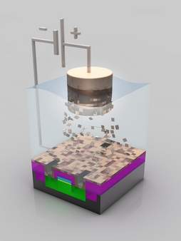
'Wafers' entering the stage of 'copper sulphate solution' at this level. Copper ions are stored in a transistor through a process called 'Electroplating'. Copper ions runs from the positive terminal (anode) to the negative terminal (cathode). 


Copper ions have a thin layer on the surface of the 'wafers'. 


Mashed excess material, leaving a very thin layer of copper. 


Well already started complicated. Much is made of metal layers to interconnect the various transistors. How is this connected series of relationships, it is determined by the architectural engineering and design teams that develop the capabilities of each processor. Where computer chips look very flat, it actually has more than 20 layers to create complex circuits. If you look with a magnifying glass, you will see a complex network of circuits and transistors that looks futuristic, 'Multi-Layered Highway System'. 


This is just a super small sample of the 'Wafer' is going through a phase of the first test capability. At this stage, a test pattern is sent to each chip, then the response of the chip will be monitored and compared with 'The Right Answer ". 


After test results showed that the 'Wafer' pass, 'Wafer' is cut into a section called 'Dies'. Try the skipper can see, the process was really complicated, but the result was a small talaga. In the leftmost picture that there are 6 groups 'Wafer'. 


'Dies' which passed the test, will be included into the next stage of the 'Packaging'. 'Dies' which does not pass, thrown away. 


This is a picture of the 'Die', which had been cut earlier in the process. 'Die' in this picture is the 'Die' from the Intel Core i7 Processor. 


Undercoat, 'Die', and 'heatspreader' fitted together to form the 'Processor'. Green bottom layer, used to form electrical and 'Mechanical Interface' for the processor in order to interact with a PC system. 'Heatspreader' is 'Thermal Interface' in which the cooling solution is applied, so that the processor can remain cool in operation. 


'Microprocessor' is the most complex products in the world. In fact, to make it require hundreds of stages and which we described earlier is just that important.


During the last test for the processor, the processor in the test characteristics, such as power usage and maximum frequency.


Based on previous test results, Processor Processor grouped with the same abilities. This process is called a 'binning', 'binning' is determined from the maximum processor frequency, then the stack Processor divided and sold in accordance with the specification stable. 


Processor that has been packaged and tested, go to the factory (eg for using that Toshiba laptop) or retailing (eg in computer stores) 

 
Design by Free WordPress Themes | Bloggerized by Lasantha - Premium Blogger Themes | Blogger Templates